6 MINUTE READ
This PCB Troubleshooting Flowchart was first developed by Huntron Technical Support 25+ years ago and looking at it now is still pertinent to today’s PCB repair environment. It provides a fairly accurate window into the process many technicians and engineers follow when looking to diagnose and repair a printed circuit board (PCB).
In this article we take a closer look each step in the process and offer some suggestions that may help you with your PCB repair procedures.

The Type of Fault
In the PCB troubleshooting world you can essentially break down fault types into two categories based on the environment. Determining the type of fault will dictate the troubleshooting path you should follow.
Production Faults are problems encountered during the manufacturing of the PCB. These types of problems can be solder process issues such as solder bridges, cold solder joints, solder balls and solder voids. Other common production faults are missing components, incorrect component polarity or value and a host of PCB trace issues. Rarely would you encounter faulty components in the production world.
Field Faults on the other hand are rarely process issues but more likely problems caused by physical damage from the stress of being in the outside world. Damage from being dropped, subjected to voltage surges (lightning!), excessive heat and user abuse are common issues. In some cases it can be simply a failed component such as an electrolytic capacitor that has degraded over time although component failures are more likely to be caused by the outside stresses mentioned earlier.
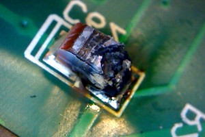
The Importance of Visual Inspection
Visual inspection may seem the natural first step to detecting what is causing the problem on a PCB but some skip this step in lieu of going straight to powered testing. This can be somewhat risky in that putting the PCB into a powered state could create more damage if it has catastrophic issues such as short circuits.
It is always important to take a close look and see if you can detect any obvious issues with the PCB. Sometimes the problem is very obvious such as a burned components but more subtle issues such as cracked solder joints can be more difficult to find. You can use a magnifier, microscope or high resolution video camera to assist with getting a more effective look at the PCB where problems can be difficult to see with the naked eye. Visual inspection will normally catch most of the issues on PCBs with manufacturing based faults.
Check for Shorts
Before trying to verify board function with a power on test, it can be a good idea to take some time and check for short circuits on the PCB. You can use a DMM and measure resistance or use a V/I (voltage-current) signature test such as a Huntron Tracker to test key points on the PCB such as voltage lines to board ground. Shorts circuits on a PCB can possibly cause more damage if it was powered on so it is worth the time to make a quick check.
Verify the Fault
This step may not always be possible in situations where you do not have a working assembly or test bed to verify the problem with a suspect PCB. If you do have a working assembly or test bed then testing the function can tell you more about the suspected fault or possibly tell you that there is actually nothing wrong with the PCB. Once the fault is verified then you can move on to troubleshooting the problem. If the fault is not verified then you may be dealing with an intermittent fault and running the board continuously (burn-in) may eventually produce the fault.
Troubleshooting the Fault
Troubleshooting a PCB generally starts with the easiest fixes first such as reseating ICs in sockets. Also look at any connectors for damaged or missing pins. If you suspect the problem might be program or firmware related, try replacing the programmed devices. If these steps do not produce a positive result then you will need to start testing to the component level.
Knowing something about the functions of the PCB may help you identify a particular section of the board to focus your efforts on. For example, if the problem with the PCB is that +5 volts measures +3 volts then you would concentrate on the voltage supply section of of the PCB or possibly voltage line filter capacitors. Of course since this is the Huntron News blog we suggest that a Huntron Tracker will be a useful tool at this point to help detect faulty electronic components. You are looking for damaged components at this step in the process so an instrument that can help you detect this damage is essential. Start with components that have a higher fatality rate such as (you guessed it) electrolytic capacitors. From there, work your way down from the most complex parts (ICs and semiconductors) to simpler parts (resistors and capacitors). This is also the longest part of the troubleshooting process since the more complex the PCB, the more time is required to find the faults. There may be a point at which the cost of troubleshooting is more than the cost of the PCB so there could be time limits put in place. If you have a higher volume of high cost PCBs to repair then including some level of automation may be a consideration.
Final Steps
Once you have diagnosed the PCB, repaired process problems and replaced bad components then the next step is to verify if your repair was effective. Test the PCB in a working assembly or test bed to learn that it is either functional or needs further troubleshooting. If the PCB works then you can choose to allow for further burn-in test making sure it functions long term or choose to return the PCB to inventory.
With the end goal being the successful repair of a faulty PCB, how you get there is entirely your decision and the simplest solution is usually the best.
Good luck and happy troubleshooting.
3 responses to “The PCB Troubleshooting Flowchart”
[…] asked for permission to share to which they granted.Lo and behold, we see that Huntron has posted a new article on their News blog that “revisits” this old flowchart but has added details about each […]
Glad you liked the update!
This is the great hub for sharing the knowledge. The flowchart for PCB troubleshooting is the best way to understand the whole concept. Thanks!