3 MIN. READ
Printed circuit boards (PCBs) can be manufactured quickly. Pick-and-place machines automate the placement of components onto the PCB, and reflow ovens eliminate the need to solder each connection separately. However, high-speed manufacturing requires a PCB testing strategy that can keep up with production. Slow testing can create a bottleneck in your facility.
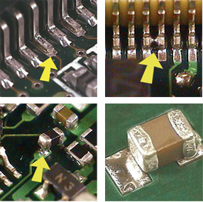
Every manufacturing process has an inherent failure rate. Placement of solder outside of the designated location can lead to a solder bridge that might be invisible to visual inspection. PCB testing is crucial to:
- Minimize waste.
- Reduce returned products.
- Optimize safety.
Without an adequate testing strategy, your business could face diminished profit margins, unhappy customers and even product liability lawsuits.
Common PCB testing strategies
There are many ways to test a PCB. However, different testing strategies provide different information at different levels of detail. Moreover, a testing strategy must account for costs in time, money and effort.
For example, a bed of nails can test several connections simultaneously. This provides a high degree of resolution but requires investment to create the test bed and interpret the results. Conversely, a functional circuit test can determine whether the PCB works but cannot isolate why the circuit does not function.
Briefly, a few of the more common testing strategies include:
In-circuit test (ICT)
These tests use probes to assess components and circuits within the circuit board. The PCB can be placed onto a test fixture that has probes fixed to touch connections on the board. Alternatively, a fixtureless ICT uses flying probes that are controlled automatically to move across the board and touch connections on the board. The benefit of ICTs is they give very detailed test data. The drawback is they require specialized testing equipment that is customized or programmed to test a specific PCB.
Between test fixtures and flying probes, fixtureless flying probes are more flexible and can be reprogrammed for different PCB designs or different testing protocols.
Functional circuit tests
Functional tests replicate the operating environment of the PCB. Typically, the PCB is connected to an electronic assembly that simulates the final product and is activated. The benefit of functional circuit tests is they are fast and require no special testing equipment. The drawback is they provide very little information except whether the PCB works.
Boundary Scan (JTAG)
JTAG (Joint Test Action Group) is a test strategy for verifying and testing PCB design typically in a manufacturing environment. Boundary scan allows for test through a test access port (TAP) that is designed into the board and can access boundary scan enabled integrated circuits (IC) through special registers. Specialized software is used to program and execute various tests that can check PCB infrastructure, interconnections and IC functions. It is an excellent method to test more complex PCBs especially those with ball grid array (BGA) devices. Boundary scan is part of a “design for test” strategy so the it is necessary to implement it at the PCB design stage.
Power-off test
Power-off test such as Voltage/Current (V/I) signature testing has some distinct advantages over tests requiring the PCB to be powered on. Sometimes referred to as Analog Signature Analysis (ASA), it uses comparison troubleshooting that makes schematics or documentation unnecessary. It provides the ability to test circuit boards that are dead and cannot be powered on. Power-off test can reduce risk to the PCB from further damage that could occur if it was powered up. ASA is also an excellent screening test to check PCBs for catastrophic problems before adding power.
Power-off test cannot test the function of the PCB however so it is primarily used to troubleshoot PCBs down to the faulty component. Once faulty components have been detected and replaced then a functional test can be performed to verify the repair was successful.
Automated optical inspection (AOI)
An automated optical inspection uses high definition cameras to capture images of a PCB and its components. A computer then compares the images to reference images. Boards that show any anomalies are set aside for further inspection and repair. The benefit of AOI is that it is faster than manual visual inspection.
Automated X-ray inspection
Automated X-ray inspection uses the same X-ray imaging that is used in medical applications. As you might expect, automated X-ray inspection can look for defects that are not visible to the naked eye. X-ray images can reveal voids inside solders and missing solder connections, solder bridges, and components. Automated X-ray inspections require specialized testing equipment and can create a potential hazard in the working environment. However, these tests reveal information about a PCB that cannot be obtained in any other way.
Choosing a PCB testing strategy
Whether your business is an OEM or a contract manufacturer that supplies OEM parts, the PCB testing strategy you choose could determine your business’s reputation for quality control. The goal of a testing strategy is to choose tests that are accurate, detailed enough to distinguish repairable bugs from unrepairable defects, and inexpensive enough to meet the market’s pricing demands. With these tests in place, your business can produce high-quality parts at the right price.
Huntron Inc. has been manufacturing PCB test instruments for 44 years. Please contact us to learn more or request a demo today.
2 responses to “PCB Testing – The Benefits and Drawbacks of Common Strategies”
This is an excellent article about testing strategies.
Have considered adding JTAG boundary scan solutions to your list of testing strategies?
Please continue these informative 3 minute reads!!!
Thank you,
It would be useful to add JTAG to the list. Thanks for the input!