3 MIN. READ
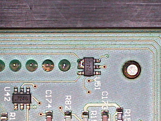
Printed circuit boards (PCBs) can fail for many reasons during manufacture and use. These PCB problems must be detected and repaired to minimize waste and reduce costly product recalls.
Good testing equipment and sound testing protocols are necessary to detect these PCB problems at the factory before assembly or after the product malfunctions in the field. Your protocol and testing equipment must be designed to detect the most common PCB problems that your products could encounter.
Design flaws
Poor PCB design can lead to open circuits, short circuits and heat damage. Design problems could lead to:
- Acid traps: If traces are laid out at sharp angles, etching acid can become trapped at the intersection and eat away the conductor. This leaves an open circuit in your PCB.
- Narrow traces: When PCBs include narrow traces, the thin metal conductor can break or wear off the PCB, leaving an open circuit. Compounding the problem, the broken conductor can migrate elsewhere on the PCB, shorting out other components and circuits as it moves.
- Edge short circuits: If a conductor is near an edge, it can short out against conductors in other PCB layers.
- Starved thermals: If a thermal relief has insufficient space to transfer heat to the plane or a heat dissipating fin, heat will build up in the PCB and damage solder joints and electronic components.
Unfortunately, design flaws can be difficult to correct after production has commenced. The PCB will need to be redesigned, and defective products that are returned for repair will need to have their PCBs replaced with the improved design.
Soldering flaws
Soldering is so critical to electronic devices that the IPC, a committee that sets global standards, established the soldering standard referred to as J-STD-001C. This standard defines both the methods used to produce compliant solder joints and the techniques used to verify solder joints meet the standard.
Soldered joint flaws can take many different forms. However, the problems that result fall into two categories:
- Open circuit: The solder fails to provide a physical and electrical connection between the component pin and the PCB pad.
- Short circuit: The solder provides a bridge to a different component or pad.
You can correct soldering defects by repairing the defective joint. However, you need testing equipment to identify the bad joints causing PCB problems.
Component failure
Defective or damaged electronic components can cause issues. In addition to replacing failed components, a manufacturer would need to identify the source of defective components or determine how the components were damaged. Your investigation might lead back to a design flaw, soldering flaw or manufacturing problem.
Age and physical damage
Heat, dust and natural material decomposition can cause PCBs to malfunction. For example, humidity inadvertently introduced during PCB manufacture can vaporize at normal operating temperatures. This vapor can push the layers of the PCB apart in a process called delamination. Delamination can also result from thermal stresses introduced into the PCB base material during manufacture. Most delamination issues can be solved by observing proper PCB storage protocols.
The operational life expectancy of a PCB is generally determined by its ability to handle heat. Even at normal operating temperatures, thermal cycling that occurs as the PCB heats and cools will introduce thermal stresses into the board. This can crack the base material, break joints and alter the chemical makeup of traces.
These problems will usually require a complete replacement of a PCB rather than PCB repair.
Testing to find PCB problems
Huntron Inc. sets the standard for power-off PCB testing equipment. Using sound testing protocols and the right equipment, you can quickly identify the most common PCB problems.
To schedule a demonstration or request a product quote, contact us today.
Meta Title:
Most common PCB problems and possible solutions
Meta Description:
PCB problems include poor designs, defective components and accumulated damage from thermal cycling. Learn how to identify these problems and some possible solutions.
Meta Keywords:
PCB problems
One response to “Most Common PCB Problems and Possible Solutions”
Thanks for helping me understand that it can be hard to correct errors in the process. So it would probably be best to have professional PCB solutions that a company can trust to ensure that there will be no materials and time wasted in the process. It can save the money as well because they can keep materials from being wasted which means that they won’t have to buy new items for the project.